

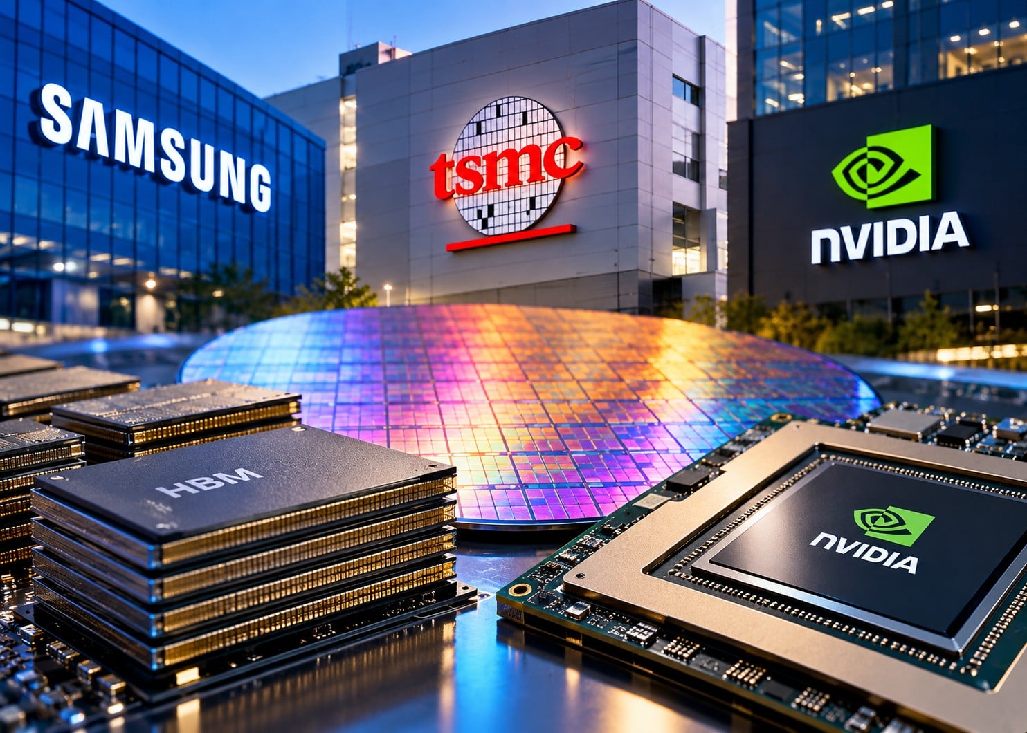
Samsung Electronics will reportedly use manufacturing technology from TSMC to produce a key component of next-generation high-bandwidth memory for Nvidia, bringing three of the world’s most important AI-chip suppliers into the same advanced memory supply chain.
Samsung plans to use TSMC’s 3-nanometer process to manufacture base dies for Nvidia’s next generation of custom HBM products.
The reported arrangement would mark the first time Samsung has used TSMC’s advanced 3-nanometer technology for this stage of its HBM production.
HBM has become one of the most strategically important components in artificial-intelligence computing. Unlike conventional memory, HBM places memory components in tightly integrated stacks capable of moving enormous quantities of data rapidly between memory and AI processors.
That bandwidth is essential for training and running increasingly large artificial-intelligence models.
The reported cooperation is particularly notable because Samsung and TSMC are major competitors in advanced semiconductor manufacturing. But modern AI systems increasingly depend on specialized technology from multiple suppliers.
A single advanced accelerator can involve processor architecture, foundry fabrication, high-bandwidth memory, advanced packaging, networking and power-management components produced by different companies and sometimes in different countries.
The arrangement would also be important for Samsung. Its semiconductor business is benefiting from an extraordinary AI-driven memory cycle, but competition for the most advanced HBM business remains intense.
The development moves beyond the earnings strength recently reported across the semiconductor industry and into the architecture of Nvidia’s next-generation memory supply chain.
Investors should watch for confirmation from the companies, the timing of production and whether the arrangement expands as Nvidia moves toward increasingly customized memory designs.